Philips PM 3265 Repair
This post was the first post of my first attempt at a blog (which was never published). Albeit I since re-wrote it completely, I decided to keep its original date, which consequently now predates the date this site went online.
I still like analogue scopes. Although the convenience of a digital scope’s features is hard to be matched, I still like to come back to the older world from time to time. Why? I have yet to meet a DSO which is as satisfying to operate as even a basic analogue scope. On a DSO, no matter the price point, you always notice there’s software handling your input, given the ever so slight lag. Not to mention the overall haptics; rotary encoders and rubber push buttons just don’t compare to the real deal.
From all my analogue oscilloscopes, the PM 3265 is my favourite one. 150 MHz bandwidth are more than enough for most purposes and alternating timebase mode is one of the best ideas ever (no, not a delayed switch in time bases like everyone else seems to do it). Did I mention it has a multiplier? I have never seen another analogue scope with a built-in multiplier.
I bought this particular scope used and mostly untested on eBay. As far as ‘untested’ goes, the fault it has was fairly mild, so this repair post can be rather short.
The erroneous behaviour
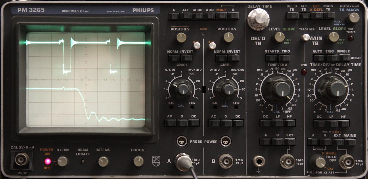
One of the two channels did weird things. I connected a pulse generator to both channels and stepped to a few frequencies. The next ‘screenshots’ show the response for each case, with the good channel on top and the faulty on on the bottom.
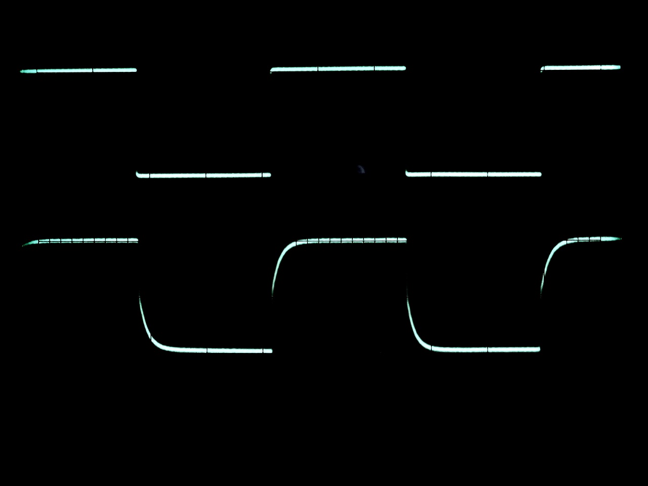
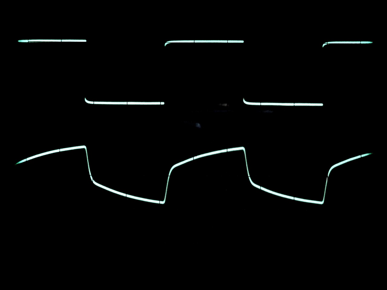
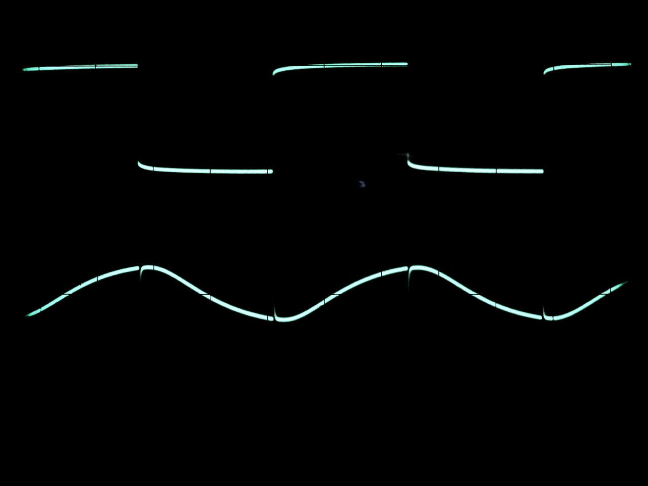
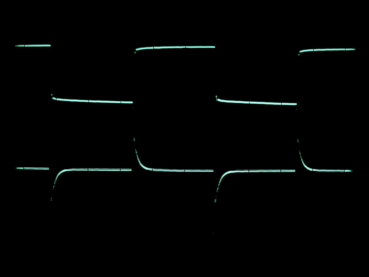
The behaviour didn’t change when switching the horizontal or vertical deflection and was mostly independent of input amplitude. That’s why the figures don’t denote the vertical scale (I didn’t write that down, and, to be fair, it was adjusted between the measurements at different time scales).
Taking a closer look
The covers on top and bottom are easily removed. As soon as that’s done, you’ll notice the thing is packed. Worse, it’s packed with bloody ceramic hybrids.
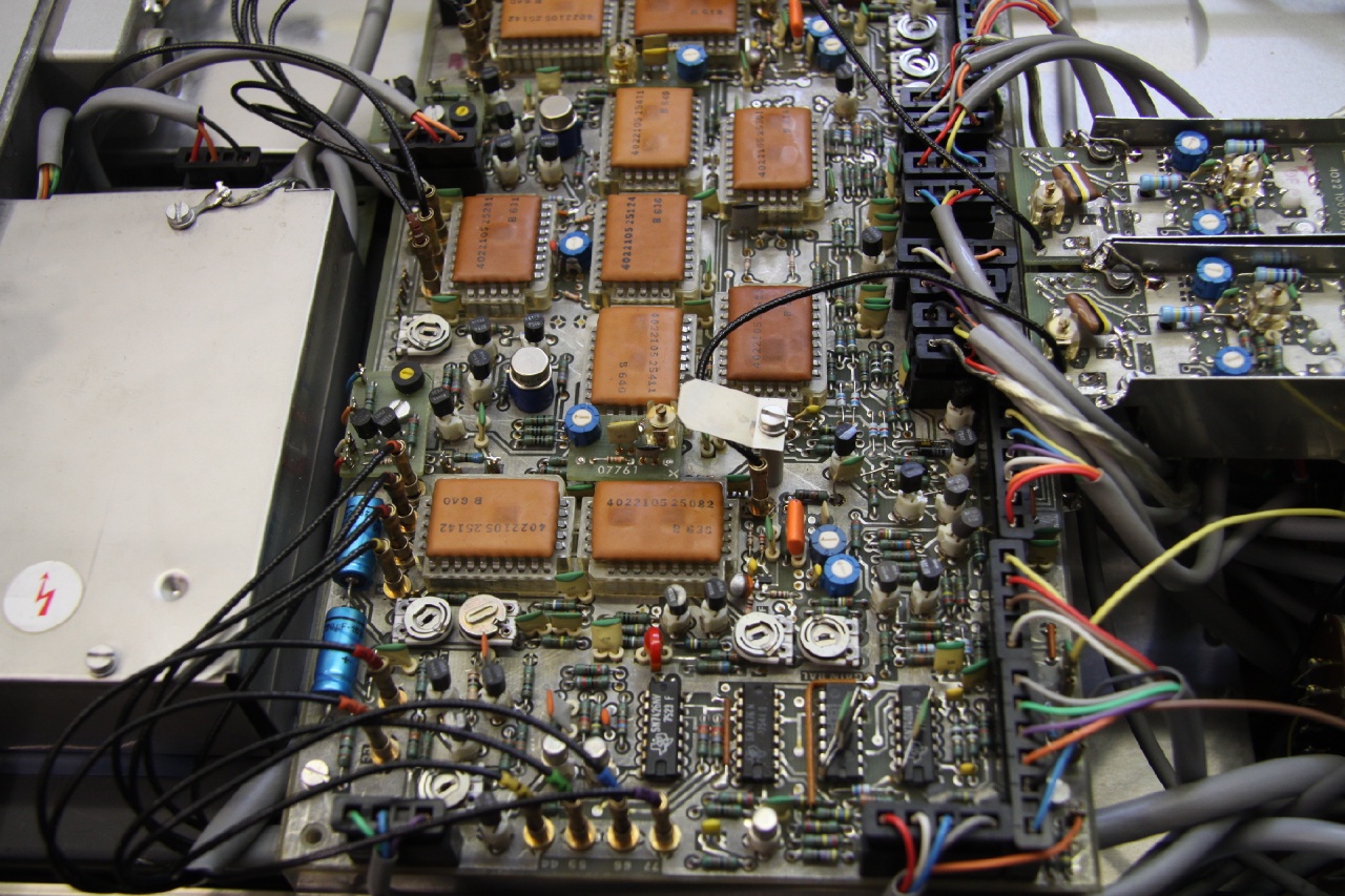
One can only hope that the culprit isn’t one of these. Although the service manual (which I was lucky to have) shows the inner circuitry of each of these blobs, I don’t want to find out how much that helps.
After tracing the input signals about around the instrument, I concluded that the problem has to lie within the input amplifier. These are separate, shielded blocks which can be seen to the right on the image above. They seem to be mounted to the front panel:
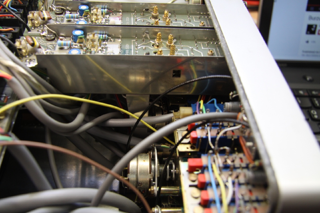
The input amplifiers needed a special tool for removal, as they were screwed to the front panel with a recessed, special nut. I quickly filed one from a distance bolt (not shown). The rectangular hole, in case you are wondering, is for the front cover and serves no purpose in operation.
Diving into the input amplifier
As I mentioned, I was lucky to have the full service manual. That means you can have a look at the schematic and have a go at figuring out where this weird behaviour comes from! If you’re here for the puzzle, this is your chance to stop reading.
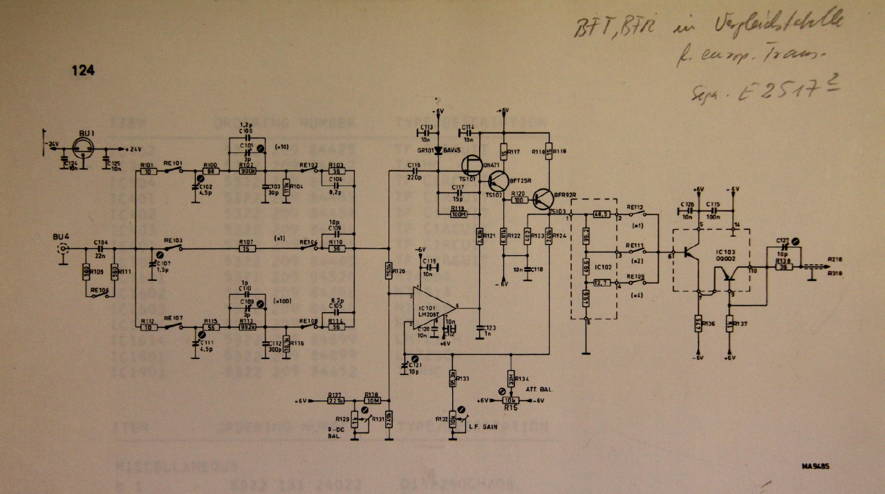
With no dependence on the input range, the left part of the schematic with the switchable voltage dividers and the coupling selector can be ruled out. Next up in the signal path is the first stage of the input amplifier and here’s where our problem will turn out to be. So, let’s have a closer look!
The first thing to note is that the first stage is a split-band amplifier, i.e. high- and low-frequency contents of the signal are fed through different circuits before being reunited shortly after. Here, IC101 is responsible for the low-frequency part, including DC. The necessary low-pass filter is not immediately obvious: The op amps frequency compensation is used here, with a unnecessarily large value for C120. IC101’s output is fed as a (relatively) DC bias into the simple voltage follower with TS101. TS101 is only coupled with a 220 pF capacitor to the input, so that’s where our high frequency signal is passing through the circuit. The resistor divider connected to TS103’s emitter feeds back the output voltage to the op amp and closes the loop for the low frequency amplification. Both paths will have an overall voltage amplification close to 1, but provide a significant current amplification to drive the subsequent circuitry.
There must have been a really good reason to choose this design, as getting the frequency response straight surely involved a lot of work. A flat frequency response is kind of critical after all for an oscilloscope input, isn’t it? I’d guess this approach was necessary because the temperature dependency of a discrete JFET voltage follower was too high and a matched JFET pair was out of the picture for some other reason.
As it turns out, TS101 was the culprit. Going back to oscillograms at the start of this post: At low frequencies, you notice the marred edges of the square wave, pointing to the missing hih frequency contents. At 50 µs/div, this becomes more noticeable and at 5 µs/div even more so. Here, some spikes begin to appear, though, and at 500 ns/div these are all that’s left of the signal. Without TS101, the high frequency path is only coupled through C117, a 15 pF capacitor. With the low frequency path almost completely silent, only the capacitively coupled peaks at the square wave’s edges appear at the output.
I found the BFT46 as a suitable alternative to the no longer available ON471. Interestingly, it looked like the transistor had already been replaced at some point in time (notable flux residue around it). So maybe that’s where the handwritten note on the schematic originated from?