Pb Power bank

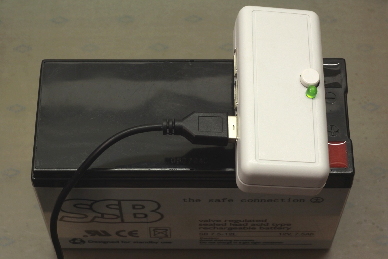
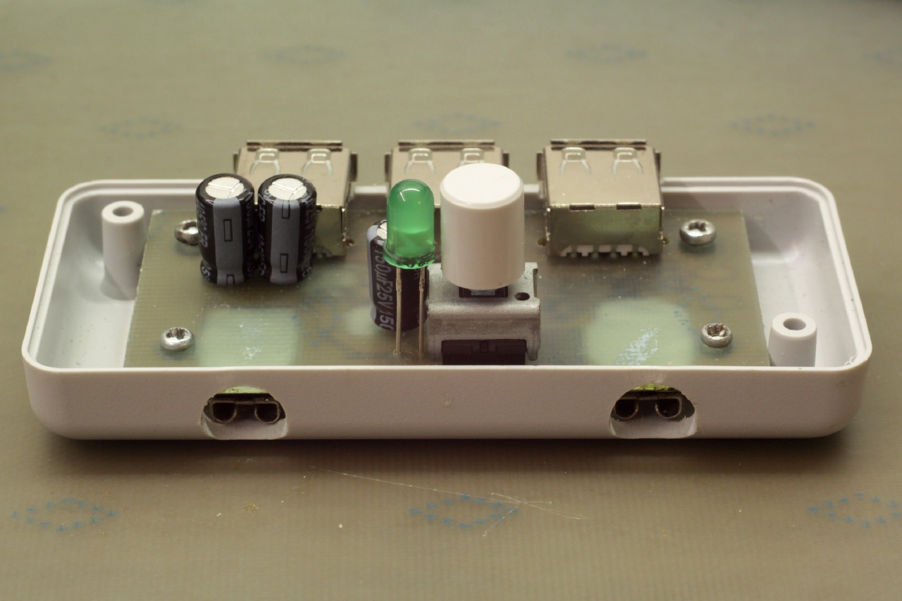
In preparation for being off-grid for a few days, I quickly built this ‘power bank’ around a 12 V 7 Ah lead gel battery. The circuit is simply pushed onto the battery’s 6.3 mm contacts and provides 3 USB ports. Charging circuitry is not included but the battery terminals are still accessible anyway.

The schematic, with the MCP16322-based buck converter and a LM393 with TL431 reference for under-voltage lock-out and over-current protection. The schematic, with the MCP16322-based buck converter and a LM393 with TL431 reference for under-voltage lock-out and over-current protection.
The switching regulator around a MCP16322 is as basic as it gets. A dual comparator adds a deep discharge protection and a over-current shutdown.
The bottom of the PCB, which has no solder mask. Visually dominating are a few large solder joints for the mechanical pins of the USB jacks and the 6.3 mm connectors (which are just regular crimp connectors originally made for cables). The main buck regulator IC is a tiny QFN near the centre of the PCB, surrounded by a slightly larger SMD inductor and a few capacitors. The top-mounted USB jacks can be seen protruding from behind the PCB at the bottom of the picture.
The overcurrent shutdown was, however, a bit over-sensitive. After trying to fix it with additional ground connections (the layout is only single-sided and thus suboptimal, after all), I finally disabled it by shorting R10. The buck converter is still protected by its current mode operation.

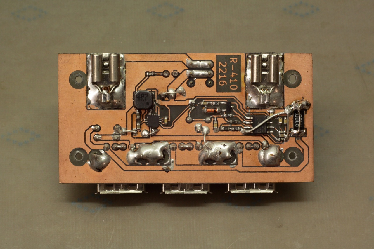
KiCad schematic and PCB layout can be found here.