A short reflection on direct laser PCB printing
I have been using a Lexmark E360d laser printer modified for depositing toner as an etch resist directly to PCB material for a while now. Details about the build have already been available on the project’s git repository, and this I’d like to focus on some comments on the actual usefulness of the project. PCB manufacture has been decreasing in its price, so I rarely use the ‘haxmark’ any more. It gets reactivated when I need a board fast and then it still does a decent job.
The general idea
The ultimate goal is to be able to etch the PCB as straight as possible from the printer. I use regular copper-clad PCB material without photo resist, so ordinary toner will have to be the etch resist. To deposit it, the laser printer has to modified: it should print on the PCB just the way it would on paper. Regular toner is really durable, so there won’t be any surprises when the PCB is submerged in chemicals.
From a mechanical point of view there are quite some modifications to be made. Because PCB material is a lot thicker and more rigid than paper, the printer’s feed mechanism won’t work as intended until large parts have been removed. Instead of being bent around internally, the PCB material is placed on a thin metal carrier which is pulled in at the front and ejected straight through a newly cut slot on the back. The optics and drum are still in place and the toner is directly transferred onto the copper.
Because a lot of the mechanics are missing, a lot of sensors are, too. Normally, the printer’s brains will get signals as the paper is passing through the internals and will stop everything when something unexpected happens to avoid damage. Thus, if the printer should actually print and not only produce paper jam errors, these signals need to be simulated. A small PCB with a microcontroller functions as a replacement for all the removed mechanics by feeding all expected signals to the printer’s main PCB.
Additionally, the printing process has to function without a fuser. It wouldn’t provide enough heat and certainly have problems with the thickness of PCB and carrier. The PCB exits the printer with the toner particles stuck on solely by electrostatic forces. Those are stronger than you might think (even blowing across the PCB isn’t a problem), but obviously not string enough for the etching process. A simple solution is to place the PCB in acetone vapour. That doesn’t degrade the printing quality at all but effects great durability as it ‘sets’ the toner particles by solvating it slightly.
And that’s pretty much all it takes! Etching works as it always does, but the process before it is greatly simplified.
The process step by step
I design my PCBs in KiCad, but the CAD program, of course, doesn’t really matter. These are my steps for etching a PCB from start to finish:
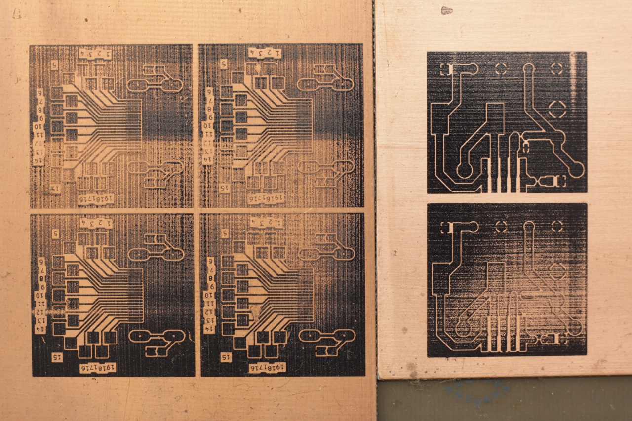
- I export the copper layer as PostScript and run a hacked-together script to align the PCB in the upper left hand corner of a DIN A4 page, with an empirically determined margin. Otherwise, the position of the PCB in the CAD program’s drawing area would matter and double-sided PCB would be impossible to get aligned.
- I choose a piece of copper-clad PCB material and straighten it by bending it back and forth.
- The copper surface gets a clean-up with abrasive cloth before wiping copper dust and other residues away with some acetone. I also take care of any sharp edges which would otherwise damage the drum over time.
- I attach the PCB material to the carrier with a piece of copper tape along the top edge. I use 5 mm wide tape, but that doesn’t really matter as long as it attaches the PCB well and doesn’t get in the way. Strictly speaking, there needs to be a connection between carrier and copper surface so the electrostatics can work. Yet, I found regular copper tape with no conductive glue sufficient (it doesn’t insulate that well).
- Printing works as usual from the PC side. The carrier is placed where the rollers can grab it and with a push of the ‘OK’ button the print is started. After the carrier exits the printer, I inspect the PCB for any obvious flaws.
- I place the PCB in a small closed container with a bit of acetone in it. The PCB is elevated, so that only acetone vapours can reach it. After a few minutes, the toner is hardened sufficiently.
- Inevitable small inaccuracies can be corrected with a permanent marker and the PCB is ready for etching!
For double-sided PCBs I just do the whole process a second time after covering one of the copper surfaces with wide tape while etching. It would be possible to etch them in one go, but I didn’t bother (yet) to build a jig for holding the PCB in the acetone vapour so the previously printed side won’t be marred.
Pros and cons
This process isn’t perfect. If you are thinking about converting a printer for this job, my experiences might help you in your decision.
What works well:
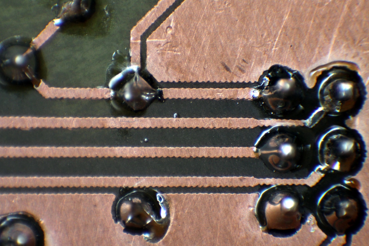
- The resolution is great. Structures as fine as 5 mil are no problem. Tolerances are no problem either.
- The toner is very durable. I thought about using it for printing on metal control panels.
- The alignment for double-sided PCBs isn’t harder than with UV exposure and photosensitive PCB material. I added a small piece of sheet metal for alignment onto my carrier which makes this a lot easier.
- You see clearly what’s going to be the result after etching and you can fix things before it’s too late. Either it’s black, or it isn’t. No in-betweens and no guessing as with UV exposure.
- And, of course, its fast.
Where there’s room for improvement:
- The printer’s drum is delicate and you should watch out for sharp edges or you won’t have fun with it for long.
- Similarly, the opening in the printer’s back has to be covered, otherwise stray light will ruin the drum over time.
- It is more sensitive than I thought to unevenness in the PCB material. This is the largest problem for me because even small differences lead to holes in the print and practically all PCB material I have is badly warped. When etching, I spend most of the time bending PCB material to get it straight.
- It needs a conductive surface. If you thought you could use this for silkscreen on a single-sided PCB, nope, sorry.
For my use case, the pros outweigh the cons. I still have all the stuff for UV exposure of photosensitive PCB material around but I haven’t used it since I built the ‘haxmark’.